Detail machine
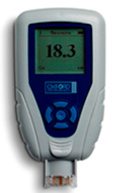
Copper Plating Gauge - CMI165
Product Use
CMI165 is the first domestic replacement handheld copper thickness tester to be launched.
It accurately grasps the needs of customers in the circuit board industry and
provides a highly competitive and economical alternative used for PCB.
FPC before and after opening, drilling, plating, etching and other processes before
the relevant copper foil thickness detection.
Product Features And Parameters
♦2Point calibration and multi-point calibration, no need to switch files to achieve accurate measurement of copper thickness in a wide range.
♦Measure The bending arc of the test head and screen ,are easy to observe.
♦Can be replaced The probe can be replaced, economical and practical.
♦Test range: 2-254um (0.1-10mil)
♦Unit: Data display unit can be selected as mil or um.
♦Operation language: English, Chinese.
♦Multi-point calibration, accurate coverage test of thick copper plate.
♦Test mode: Single and continuous measurement modes can be selected.
♦Display: TFT2.0LCD display,240x320pixels
♦Test accuracy: ±3%, with temperature sensing.
CMI760 Benchtop Copper Hole/Surface Copper Thickness Gauge
Product Use
Desktop dual-function thickness gauge for measuring copper thickness on PCB plated hole surfaces.CMI700 & MMS® PC2
Product Features And Parameters
♦ 7-inch touch color screen, easy to use operation interface,
♦ With hole copper probe ETP, it can measure the aperture above 35mils.
♦ Temperature compensation function, the measured data is highly stable.
♦ Application: Eddy current induction measurement of PC B hole copper thickness; micro-resistance measurement of PCB surface copper thickness.
♦ 99 groups of application programs, which can set hole copper or surface copper correction program groups independently.
♦ The correction factor and compensation value can be set separately to meet product specifications and standards.
♦ The upper and lower limits of specifications can be set separately to facilitate the calculation of Cpk and identify whether it exceeds the measured range.
♦Unit of measurement: mil,um,mm,inch.
♦The copper probes for hole surface all adopt the replaceable probes with unique design.
♦The test head adopts the quick plug-in connector design
♦Measurement Range:0.01-20.0mils (0.2-500um ) Hole Cu:0.04-8.0mils (1.0-200um ). ♦Minimum hole size ETP: 0.35mil (0.85mm) or more
♦Tolerance ±3% (according to standard film).
♦Resolution SCP-15:0.001mil (<mil)/0.02mils (>lmil), ETP: 0.01mils(0.25um).
♦PCB thickness limit SCP: none, ETP: minimum 30mils(0.75um)
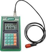
Handheld copper hole gauge thickness milum/mm610
Product Use
Milum SeriesM M 610is a handheld measurement PCB Thickness measurement of through-hole copper plating instrument.
Product Features And Parameters
♦Measurement PCB Board thickness30milor more, hole iameter35milor more The thickness of hole copper plating can also be measured before and after etching.
♦ ETP is a special test probe for hole copper thickness measurement. It adopts a special separate and replaceable probe design, which not only has precise stability, but also is convenient and economical
♦LCD with backlight display type
♦ unit: mils and um.
♦ Includes USB connection to computer for data statistics .which can be connected to a computer for data statistics.
♦Measurement range: 0.04-4.0mil (0.5-102um).
♦Error tolerance: ±3% (standard specimen) measured product ±5%.
♦Min hole size: 35mil (0.9mm).
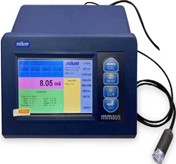
PCB Through-Hole & Copper Surface Measurement Gauge milum/mm615
Product Use
MilumSeriesMM615is a handheld measurement PCB Copper plating thickness thickness gauge.
Product Features And Parameters
♦With automatic temperature compensation function, the correction factor can be set ,Compensation t, to comply with product standards.
♦The measurement data is extremely precise and stable.
♦The measurement mode is micro-resistance type for rapid measurement of surface copper thickness
♦LCD with back light display type.
♦Unit :mil , um.
♦Standard film correction.。
♦Has USB transmission interface and statistical software, which can be connected to a computer for data statistics.
♦Range0.01-12.8mil (0.25-325um )。
♦Tolerance: ±3% (According to the standard sheet)The test product is ±5%.

Metallographic Microscope YT-JX-01/02
Product Use
It meets the professional needs of industrial testing and metallographic analysis, and is widely used in various types of semiconductor silicon wafer testing, materials science research, geological mineral analysis and precision engineering. PCB Slice analysis and other subject areas.
Product Features And Parameters
♦Adopting flat-field achromatic optical system and epi-Koehler illumination system, the image is clearer and the field of view contrast is better. The required report can be automatically generated, and the measurement magnification is automatically switched with the rotation
♦The size of any geometric figure on the plane can be measured.
♦Various geometric dimensions can be marked on the actual workpiece in the real-time image.
♦Photographs of the real object can be taken, including the marked dimensions.
♦Input lines in polar coordinates: standard line segments can be input in polar coordinates according to customer needs.
♦Optical system: finite distance chromatic aberration correction optical system.
♦Eyepiece: PL10X.
♦Objective: 5X, 10X, 20X, 50X, Optional 100X.
♦Double Mechanical moving stage, Setup1, 180x145mm,
mobile range76mmx50mm
♦Reverse Radial Kolar lighting, adaptive wide voltage90V-24V, 6V/30WHalogen lamp, continuous adjustable light intensity.
Reverse Radial Kolar lighting, adaptive wide voltage90V-24V, 6V/30WHalogen lamp,.
Camera CCD: 6.3 million pixel USB3.0 microscope camera, SONY photosensitive chip.
♦Coarse and micro Coaxial adjustment,
Total stroke 28mmFine adjustment
accuracy:0.002mm
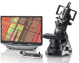
3D microscope VHX
Product Use
The fifth-generation operating system mechanism integrates observation, photography, and measurement to minimize operator fatigue. The modular component design allows for free combination of system functions to meet3Dmultiple angles. Observation, measurement, widely used in electronics, new energy related fields.
Product Features And Parameters
♦ Subtle unevenness is clearly displayed and is close to the observation image of SEM
♦Adopts high-resolutiontfRlens,4K CMOS
and the dedicated design of illumination structure, realizing a new observation method
♦Can measure the size of any geometric figure on X, Y, Z.
♦Optional observation method: multi-directional lighting
change analysis.
♦ 20to6000times automatic”Seamless scaling”
♦Lens gradient; high resolution up toNA0.9“High resolution lens
♦There are automatic platform and electric platform rack options.
♦Equipped with 3D profile measurement and roughness measurement
(resolution 0.1um)
♦Built-in light source life4000tf
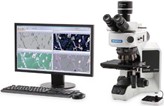
Metallographic microscope Olympus/BX53M
Product Use
It meets the professional needs of industrial testing and metallographic analysis, and is widely used in various types of semiconductor silicon wafer testing, materials science research, geological mineral analysis and precision engineering. PCB Slice analysis and other subject areas.
Product Features And Parameters
♦The modular design gives users the flexibility to build a system that meets their special requirements.
♦ UIS2Infinity optical system
♦Stage travel25mm,
♦Replaceable5Hole/5Hole coding/6Hole/7Hole/7Hole coded nosepiece
♦Objective: 5X, 10X, 20X, 50X, Optional 100X.
♦ Auto report
♦Camera, DP Series 600/800/2000 pixels
♦Camera softScanning Electron Microscope ISP/SS-60/150
ware: Optional depth of field fusion/photo Mosaic
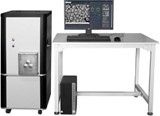
Scanning Electron Microscope ISP/SS-60/150
Product Use
Products are widely used in various industries, such as: scientific research, academies, zoology and botany, materials science, archaeology, geology and mineralogy, chemistry, physics, criminal investigation, food industry, metallurgical industry, semiconductor industry, electronics industry, ceramics industry , biopharmaceutical industry, environmental protection industry, new energy, etc
Product Features And Parameters
♦The magnification is6W/15W times optional;
♦Acceleration voltage5KV, 10KV, 15KV, 20KV, 30KV optional, high image resolution;
♦Optional selective assembly EDS;
♦High/low vacuum configuration can shorten the pre-treatment process
High/low vacuum configuration;
♦Can Look inside the stage with CCD camera;
♦Resolution: 15nm (30KV, SE Image) 20nm (30KV, BSE Image) 0
♦Image detection: secondary electron image (SE), backscattered electron image
Image detection: secondary electron image (SE), backscattered electron imag (BSE), Multi Detector (SE + BSE). ♦Detector type:SE Detector/BSE Detector.
♦Automatic functions: automatic start, automatic focus, automatic brightness and contrast adjustment.
♦Image storage format: BMP, JPEG, PNG, .
♦Software function: Like file opening, editing, storage function, length, area, angle measurement function, setting parameter initialization, image shooting mode conversion, etc.
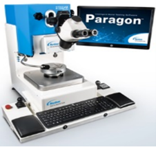
Multifunctional push and pull machine
Multi-purpose thrust machine YT-LB8100
Product Use
Multifunctional push-pull force testing machine is widely used in LED packaging testing, ICsemiconductor packaging testing, TOpackaging testing, IGBT power Module packaging and testing, optoelectronic component packaging and testing, automotive field, aerospace field, military product testing, testing of research institutions and various types of Applications such as testing research in colleges and universities.
Product Features And Parameters
- Size : 650mm*600mm*760mm (including left and right operating handles)
- Weight : 80KG
- Power : 110V/220V@3.0A 50/60Hz
- Air pressure supply: 4.5-6Bar
- Microscope: Standard high-definition continuous zoom microscope(optional trinocular microscope+high-definition CCDcamera)
- Sensor replacement method: Manual replacement and auto
- Platform fixture:360degree rotation, the platform can share various test fixtures
- XYAxis screw effective stroke: 100mm*100mmEquipped with vacuum platform, it can be expanded to200mm*200mm,Maximum testing force200KG
- XYAxis maximum movement speed: The Hall rocker is used to freely control theXYaxis, and the maximum moving speed is6mm/S
- XYAxis screw accuracy: Repeatability ±5umResolution≤0.125;2mmWithin accuracy ±2um
- ZAxis screw effective stroke:100mmResolution≤0.125um,Maximum test force20KG
- ZAxis maximum movement speed:The Hall rocker is used to freely control theZaxis, and the maximum moving speed is8mm/S
- ZAxis screw accuracy:±2umCutting accuracy: Within 2mmAccuracy ±1um
- Sensor accuracy: Sensor accuracy ±0.003%;Comprehensive test accuracy ±0.25%
- Equipment fixtures: Design fixtures according to products according to samples or drawings(Factory standard set)
- Equipment calibration: Calibration fixtures and weights 1Set.
- Quality assurance: Equipment warranty2years, free software upgrades for life(Man-made damage not included)
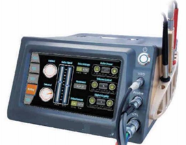
PCB/PCBA short circuit location analyzer
Product Use
The product is widely used inPCB,PCBA,SMTAfter assembly, a short circuit is found inETorICT, The instrument performs non-destructive positioning, finds short circuit points, and promptly eliminates short circuits between short-circuited components or lines. Accurately find the corresponding coordinates in the failure analysis so that engineers can conduct analysis.
Product Features And Parameters
♦ Cruise minesweeping positioning method
♦Detectable short circuit resistance range0-50Ω &0-100Ω
♦Positioning range±5mm&±3mm;
♦Detection distance0-50mm;
♦Adjustable drive peak power 0mW-3000mW;
♦Adjustable clamp peak voltage 0mV-3000mV;
♦Adjustable clamp peak current 0mA-1000mA
♦hase vector positioning method
♦Thermal resistance effect positioning method, resistance value comparison method
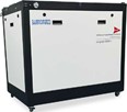
Ion contamination tester SCS lonograph series
Product Use
Products are widely used in various industries, such as: scientific research, academies, zoology and botany, materials science, archaeology, geology and mineralogy, chemistry, physics, criminal investigation, food industry, metallurgical industry, semiconductor industry, electronics industry, ceramics industry , biopharmaceutical industry, environmental protection industry, new energy, etc
Product Features And Parameters
♦The magnification is6W/15W times optional;
♦Acceleration voltage5KV, 10KV, 15KV, 20KV, 30KV optional, high image resolution;
♦Optional selective assembly EDS;
♦High/low vacuum configuration can shorten the pre-treatment process
High/low vacuum configuration;
♦Can Look inside the stage with CCD camera;
♦Resolution: 15nm (30KV, SE Image) 20nm (30KV, BSE Image) 0
♦Image detection: secondary electron image (SE), backscattered electron image
Image detection: secondary electron image (SE), backscattered electron imag (BSE), Multi Detector (SE + BSE).
♦Detector type:SE Detector/BSE Detector.
♦Automatic functions: automatic start, automatic focus, automatic brightness and contrast adjustment.
♦Image storage format: BMP, JPEG, PNG, .
♦Software function: Like file opening, editing, storage function, length, area, angle measurement function, setting parameter initialization, image shooting mode conversion, etc.
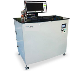
Ion contamination tester YT-LZ-01 series
Product Use
BT-LZ-01Ion pollution tester, mainly used for: surface ion concentration testing of printed circuit boards, electronic components, finished circuit board assembly, electronic and electrical equipment, etc.
Product Features And Parameters
♦Size: 28cm x28cm 65cmx35cm.
♦TestTest method: Dynamic test method/Static test method
♦Addheating device:40°C±2°C
♦Test the ratio and volume of the extraction liquid3:1&21L.
♦Measurement accuracy (F・S): ±5%.
♦Power (W): 1200W
♦ExtractionLiquid specific gravity: 0.85~0.855.
♦Environment temperature (°C): 18-25.
♦Working temperature (°C): 40±2.
♦Conductivity analysis rate (ps/cm^): 0.001.
♦Electrode resolution range (ps/cm2): 0.0001-20o
♦Conductivity Test Benchmark (MQ): 55-66.
♦Outer Shape size:1100x620xll50L (LxWxH mm)
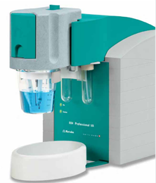
VS Plating Solution Analyzer MPC/CVS MARTIon contamination tester SCS lonograph series
Product Use
The FrenchM PCcompany provides electroplating solution organic additivesCVSanalyzers. A full range ofCVSanalyzers can analyze the circuit board electroplating process.
Product Features And Parameters
♦It has a huge potion database and is compatible with most potion suppliers on the market.
♦The software can record potential change spectra, calibration curves, and output test reports.
♦HistoricalHistorical test data can be automatically output to EXCELtable, which is convenient for users to save and trace.
♦Cleaning and automatic sample addition, multi-sample
testing module, or even VMS added module
♦Electrode design: working electrode, reference
electrode, auxiliary electrode.
♦ConstantCurrent source High current output:±1A,Pole voltage:± 15V.
♦Accuracy: ±5%
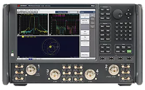
TDR Impedance Tester
Product Use
TDRThe impedance tester adopts true differential broadband sampling technology, which can automatically, quickly, batch and accurately test the characteristic impedance of circuit boards and wires and cables. It has waveform display and analysis functions and is suitable forPCBImpedance and differential loss testing of hard boards,FPCsoft boards and wires and cables.
Product Features And Parameters
♦The maximum bandwidth can reach 120GHz, is at the world’s leading level, The shortest test line length can be 1.8mm°
♦The instrument automatically calibrates when it is turned on, which solves problems such as complex calibration process and calibration data drift.
♦Inside1Set up electrostatic protection circuit, can withstand 35kVElectrostatic discharge.
♦Intelligent Test software to automatically obtain the
starting point and end of the waveform.
♦Impedance measurement range: single-ended10-100Ω
differential20~200Ω
♦Impedance accuracy: 50Ω±1%.
♦UseApplication scope: impedance strip test, in-board test.
♦Impedance resolution: 0.03Ω.
♦Number of channels:4Channels:2single-ended,1to the difference.
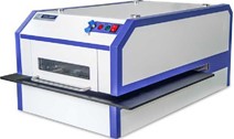
X-RayX-Ray ISP/iEDX-150WT ISP/iEDX-150WT
Product Use
This instrument is a powerful material coating/coating measuring instrument, which can be applied to coating/coating thickness,PCB/FPCgold, shackles, silver, tin, In testing fields such as gold and silver, it provides accurate and rapid analysis for product quality control.
Product Features And Parameters
♦The maximum plating detection can reach5layers.
♦Can analysis 0.2-0.5uingold layer
♦The optional alloy component analysis
function can be performed at the same time.
♦Laser positioning enables continuous and automatic multi-point program-controlled measurement.
♦Optional multi-collimator system,single collimator/
6collimator/7collimators.
♦OperationSimple, easy to learn and understand, high quality, high performance, high stability,Quickly output test results (20-40seconds).
♦GermanSi-Pindetector,SDDdetector to ensure test
accuracy.
♦DetectionDetection element AI (13) – U(92).
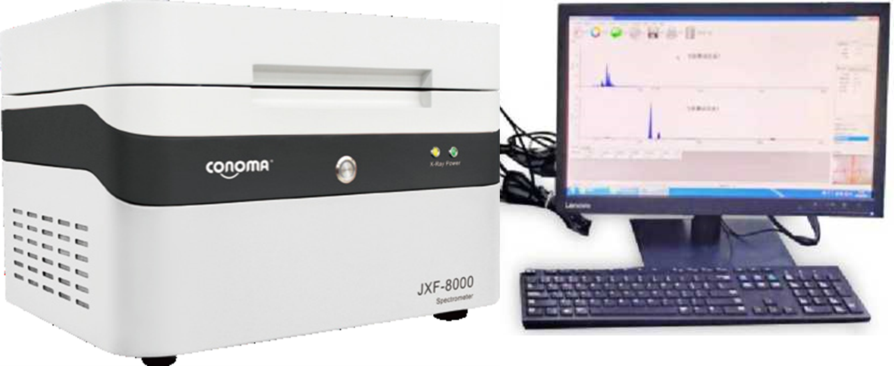
ROHS Test YT-XR-10
Product Use
YT-XR-10 is an economical, practical and easy-to-operateXray fluorescence spectrometer (RoHS,Halogen, heavy metal component) to lead (Pb), mercury(Hg), cadmium(Cd), Luo(Cr), Australia(Br), Chlorine(Cl), stele (As), selenium (Se), practice ( [ Elements such asSb) have good detection limits and accuracy. Applicable to: hardware, connectors, electronics, electrical, connectors, electroplating,PCB,plastic, leather, shoe materials and other incoming materialsROHSAnalysis.
Product Features And Parameters
♦Elemental analysis ranges from sulfur(S)to uranium(U)°
♦The elemental content analysis range isIPPmto99.99%.
♦RoHSHazardous elements specified in the directive(limited toCd/Pb/Cr/Hg/Br)Its detection limit is as high as1PPM.
♦Energy resolution is160±5electron volts.
AdoptUse American Amptekdetector Si-pin, Electric cooling instead of liquid Nitrogen refrigeration,Small size, accurate data analysis and low maintenance cost.
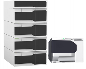
Upgraded ROHS 2.0 phthalate 4P determination liquid chromatograph
Product Use
This solution uses a high-performance gradient high-performance liquid chromatograph to measure the four phthalates controlled by the European Union in samples. It can be widely used in many analytical fields such as environmental protection, medicine, food, chemical industry, and environment.
Product Features And Parameters
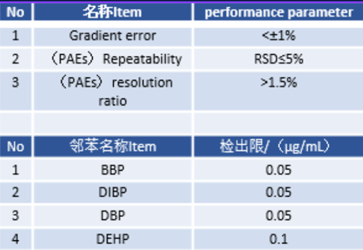
performance of machine
1.standard substance (naphthalene) is qualitatively repeatable:RSD≤0.06%;
2.standard substance (naphthalene) was quantitatively repeated;RSD≤1%;
3.Detection lower limit:BBP\DIBP\DBP≤5ppm,DEHP≤10ppm;PAHs≤0.5ppm、BPA≤0.01ppm
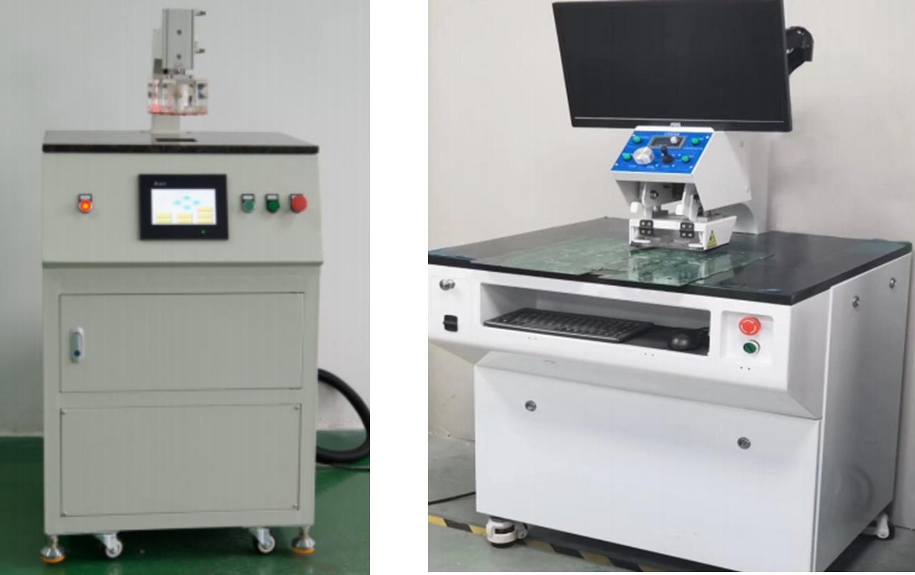
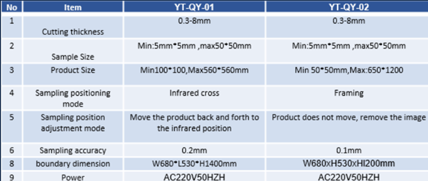
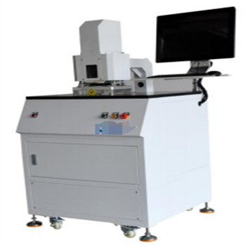
Automatic sampler YT-QY-01/02 (visual)
Product Use
YT-QY-01/02Automatic sampling machine, using the latest technology and accessories, easy to operate. This machine is used for microsection sampling required for the production process of copper clad laminates and rigid printed circuit boards and for metallographic analysis of each production process. It can be customized according to different needs.
Product Features And Parameters
Thickness measuring instrument (YT-BH-01t)
Product Use
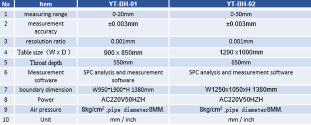
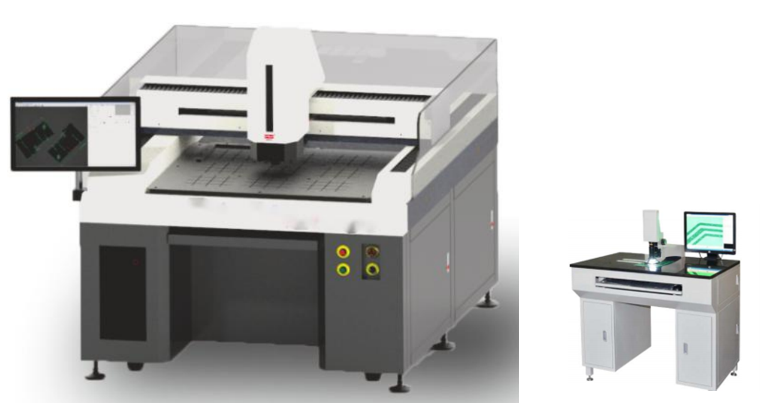
YT-BH-01long-arm plate thickness measuring instrument is mainly used for thickness measurement of copper-clad laminates and multi-layer boards after lamination, as well as the thickness measurement of other plates. It is equipped with a computer to automatically record and store the measurement data, and uses the well-known domesticSPCprocess control software to conduct a full range of process control data analysis on the measurement data.
Product Features And Parameters
Line width and line spacing tester YT-XK-01/Auto03
Product Use
Detect the upper and lower width of the printed circuit board’s inner and outer semi-finished products after development and etching (before applying green oil), the distance between lines, the diameter of round holes, blind holes, arcs and the distance from the hole to the edge, etc. . At the same time, it can be extended to the measurement ofICwafer line width and space,filmwidth measurement,LCDcircuit board measurement and other microscopic distance measurement occasions.
Product Features And Parameters
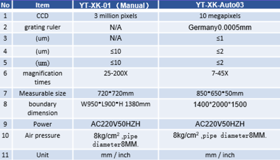
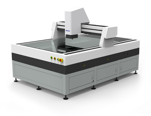
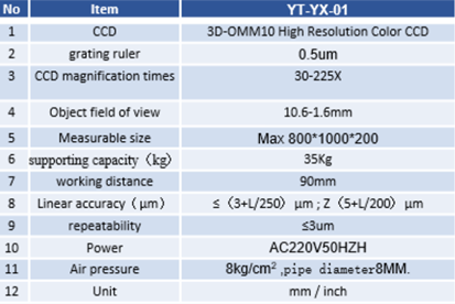
Automatic image measuring instrument(YT-YX8060)
Product Use
This product has the characteristics of high speed and precision, and can perform multiple functions on a single machine, greatly reducing the cost of repeatedly purchasing machines and the waste of space. It can efficiently detect the contour and surface shape, size, angle and position of various workpieces. Especially suitable forPCBboards, films, protective films, optical glass, electrical
It is used in industries such as sub-assemblies, large wrench parts, connectors, precision mechanical parts, electronic components, semiconductor components, etc. to achieve rapid and accurate inspection of large quantities.
Product Features And Parameters
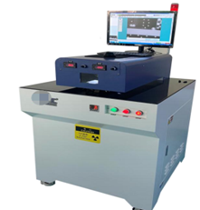
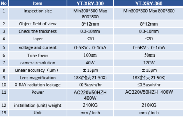
YT-XRY-360
Product Use
measurement and analysis of point-to-point, point-to-line, radius, diameter, concentricity, etc., discover process errors in advance, and avoid batch quality problems.
Product Features And Parameters
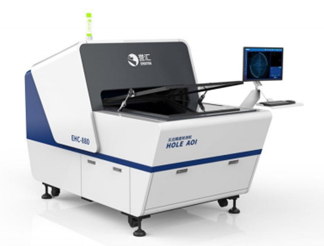
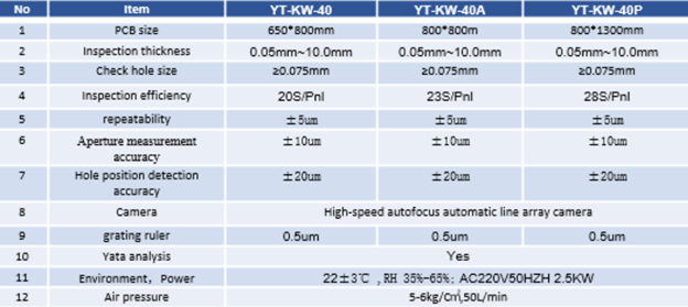
Hole AOI (YT-KW-40)
Product Use
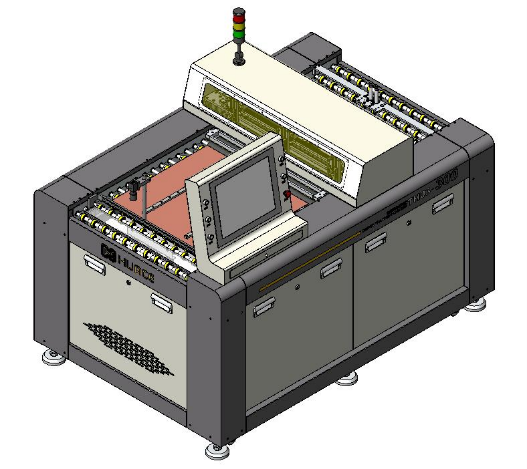
The hole position inspection machine is a device that is used to analyze the hole position accuracy after drilling PCB and generatecpk analysis reports ,and also has the function of hole inspection. It can also be used for hole inspection of soft boards.
Product Features And Parameters

YT-XRY-360
Product Use
measurement and analysis of point-to-point, point-to-line, radius, diameter, concentricity, etc., discover process errors in advance, and avoid batch quality problems.
Product Features And Parameters

Online copper thickness testing machine(YT-TH-600)
Product Use
Online copper thickness measuring machine is used in PCB production field to measure copper foil thickness after etching, electroplating, etc., to control and monitor whether the thickness of incoming copper foil meets production requirements.
Product Features And Parameters
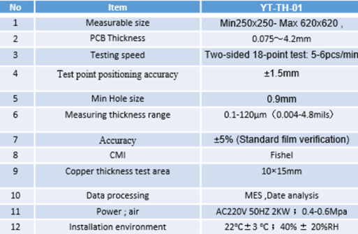
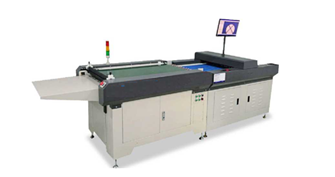
Hole counter YT-YK-01
Product Use
YT-YK-01The hole inspection machine is mainly used to inspect the through holes, component holes, slot holes, various special-shaped holes, etc. on the printed circuit board(PCB). In the printed circuit board manufacturing process, a hole inspection machine is required to ensure the quality of the holes after drilling, electroplating, tin spraying and before shipment.
Product Features And Parameters
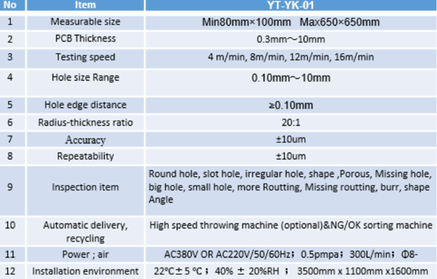

Warpage tester (YT-WQ-650/800)
Product Use
PCB Board bending and warping tester is a kind of PCB finished board or copper clad laminate board bending and warping(bowing, twisting)detection, and automatically makes OK/NG judgments and sorting based on the detection results.
Product Features And Parameters
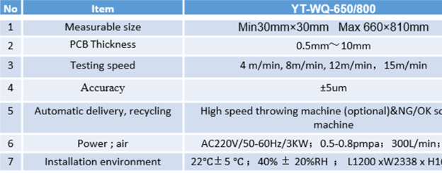
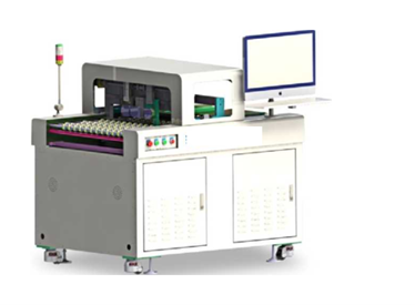
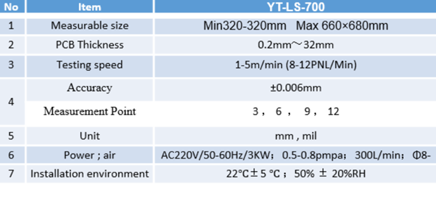
Online laser plate thickness testing (YT-LS-700)
Product Use
Applied toPCB/PCBA.Automobile, machining and other industries, Using non-contact laser measurement, it can accurately measure online PCB After lamination, sheets and plastics, Thickness of mold, etc.
Product Features And Parameters
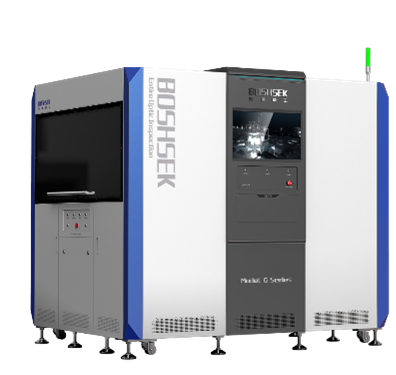
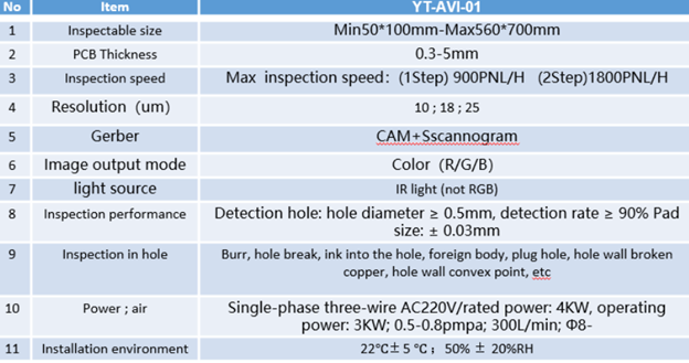
PCB Visual inspection machine (AVI YT-AVI-01)
Product Use
PCB final appearance inspection before shipping to meet customer requirements.
Product Features And Parameters
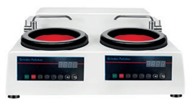
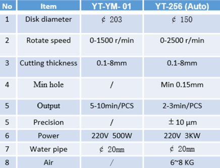
Double disc, automatic grinding machine (YT-YM-01)
Product Use
For printed circuit board physics laboratory grinding Block slices.
Product Features And Parameters
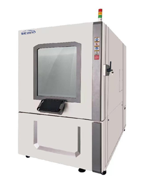
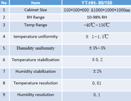
Temperature and humidity test chamber (YT-HH-150)
Product Features And Parameters
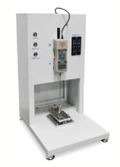
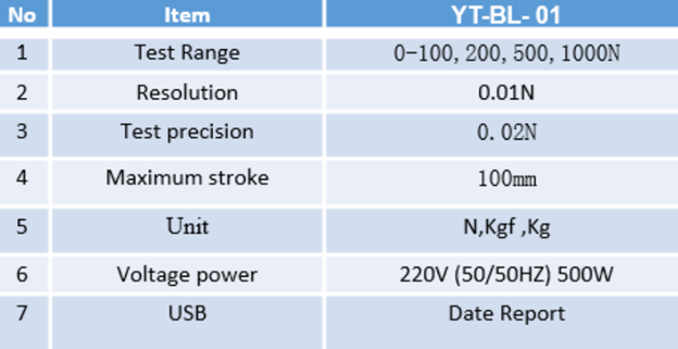
Peel strength testing (YT-BL-01)
Product Use
Professionally used to measure the rigidity/The copper foil peeling strength of the winding copper clad laminate
Product Features And Parameters
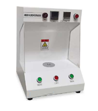
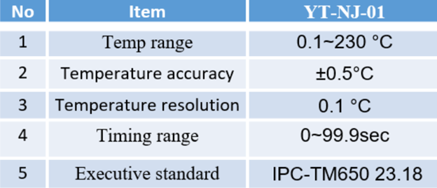
Gelation time tester (YT-NJ-01)
Product Use
professionally used to test the gelling time of prepregs and resins, and to test the gelling time of adhesive sheets used for laminating multi-layer boards to ensure that they are used in production. Raw material properties.
Product Features And Parameters
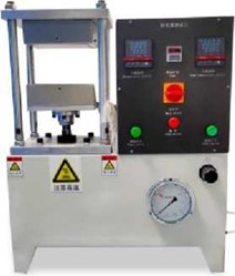
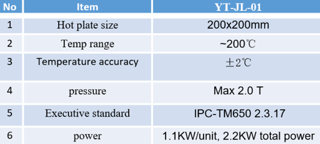
Glue flow tester(YT-JL-01)
Product Use
Resin fluidity test for measuring semi-cured sheets. Product Features And Parameters
Product Features And Parameters
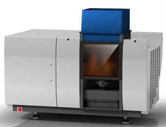
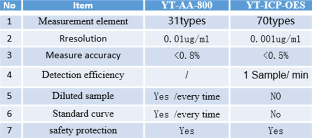
AA/ICP Machine (YT-AA-800)
Product Use
It is generally used for the determination of metal elements and some non-metallic elements in all walks of life and various samples.
Product Features And Parameters
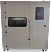
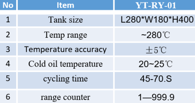
Hot oil testing (YT-RY-01)
Product Use
This equipment is a special testing instrument for printed circuit board production process control and is used for thermal shock test of printed circuit boards
Product Features And Parameters
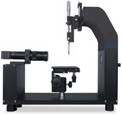
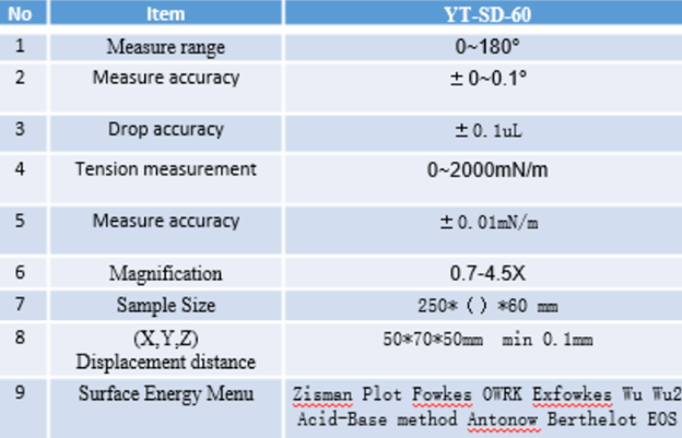
Water drop angle measuring instrument (YT-SD-60c)
Product Use
For TFT-LCD panel, PCB After ion treatment, after brushing, printing and plastic industry, IC Packaging and other cleanliness measurements, surface cleaning and adhesion quality measurements ,Hydrophilicity measurements,
Product Features And Parameters
